
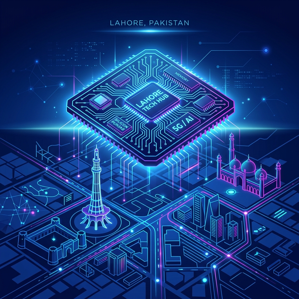
In a monumental leap for its technological ecosystem, Pakistan has officially inaugurated its first-ever Semiconductor Design and R&D Hub in Lahore. This state-of-the-art facility represents a strategic shift from a predominantly software-focused IT industry to highly lucrative hardware engineering and microchip architecture.
Backed by joint collaborations with international tech giants and local universities, the hub aims to position Pakistan as a competitive player in the “fabless” semiconductor market by 2030, capturing a segment of an industry projected to surpass $1 trillion globally.
The Strategy: Fabless Chip Design
Building a full-scale semiconductor foundry (fabrication plant) requires tens of billions of dollars and years of specialized construction. Recognizing this barrier, Pakistan’s strategy smartly focuses on fabless semiconductor design.
Instead of printing the silicon, local engineers will focus entirely on designing the complex architectures, logic, and intellectual property (IP) for next-generation microchips used in Artificial Intelligence, Internet of Things (IoT), and the automotive sector.
This initiative naturally aligns with the momentum generated by the recently established Pakistan AI Venture Fund, creating an integrated ecosystem where AI software developers work hand-in-hand with hardware architects.
Capitalizing on Global Demand
The global shortage of semiconductor design engineers presents a unique opportunity. The government hopes to train and integrate thousands of local electrical engineers into the global supply chain, significantly diversifying and expanding upon the country’s recent unprecedented IT exports surge.
“By focusing on chip design, we are entering the most intellectually intensive phase of the semiconductor value chain,” stated a senior official from the Ministry of IT. “Our goal is to incubate 50 fabless startups within this hub over the next five years.”
The Need for Uncompromising Infrastructure
Microchip design and electronic design automation (EDA) require immense computational power. Running billions of simulations to verify a chip’s architecture necessitates highly secure, unthrottled server infrastructure.
For enterprises and R&D labs pushing the boundaries of technology in Pakistan, local data processing is crucial. Nextgen Hosting provides the backbone for such high-performance computing with our Bare Metal Dedicated Servers. Featuring Enterprise NVMe storage, unmetered bandwidth, and total root control, our dedicated infrastructure ensures that proprietary hardware designs and intensive EDA simulations run flawlessly without data latency.
Looking Ahead
The Lahore Semiconductor Hub is expected to generate thousands of high-paying jobs for engineers and researchers. If successful, the government plans to launch Phase II by 2030, which will involve setting up semiconductor packaging and testing facilities—the next critical step toward hardware self-reliance in Pakistan.