
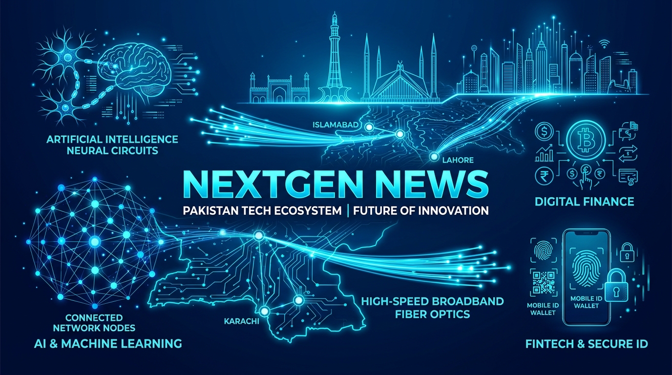
In a landmark development for Pakistan’s rapidly evolving tech ecosystem, the IT Ministry has officially inaugurated the National Semiconductor and Chip Design Incubation Center in Islamabad. This pivotal initiative is designed to position the nation as an emerging hub for microelectronics, fabless chip design, and advanced computing research, significantly diversifying its tech export portfolio.
A Vision for Global Integration
For decades, the global semiconductor supply chain has been highly centralized. However, with shifting geopolitical landscapes and an insatiable global demand for processing power—fueled by AI, IoT, and high-performance computing—new markets are being explored. Pakistan’s strategic move into chip design focuses primarily on the fabless model. By nurturing local engineering talent, the incubation center aims to design microchips that will eventually be manufactured by major global foundries.
The newly established facility provides state-of-the-art Electronic Design Automation (EDA) tools, highly subsidized incubation spaces for hardware startups, and direct mentorship from global industry veterans. The government hopes to generate thousands of specialized engineering jobs and stimulate a hardware-focused startup culture that complements its booming software sector.
The Infrastructure Behind Chip Design
Semiconductor design is a notoriously resource-intensive process. Developing intricate logic gates, simulating thermal characteristics, and running extensive validation checks requires immense computational power. Local startups and research teams must process terabytes of simulation data with zero margin for error.
To support these extreme workloads, organizations cannot rely on standard shared hosting or lightweight cloud instances. Running massive semiconductor EDA tools requires enterprise-grade bare-metal Dedicated Servers in Pakistan. For hardware startups utilizing the incubation center, leveraging robust Dedicated Servers ensures that complex simulations, verification algorithms, and synthesis processes run flawlessly, offering the raw CPU and RAM necessary to bring cutting-edge microarchitectures to life.
Strategic Partnerships and Future Growth
The National Semiconductor and Chip Design Incubation Center has already signed memorandums of understanding (MoUs) with several prominent universities, including NUST and FAST-NU, to align academic curriculums with the needs of the modern semiconductor industry. Furthermore, special tax incentives and R&D grants are being offered to expatriate Pakistani engineers working in Silicon Valley who wish to return and launch fabless ventures.
By focusing on the high-value design phase of the semiconductor lifecycle, Pakistan is taking a pragmatic and intelligent step. While building physical fabrication plants (fabs) costs tens of billions of dollars, investing in human capital and design capabilities allows the country to tap into the trillion-dollar semiconductor market with a fraction of the capital expenditure.
As the center becomes fully operational over the coming months, industry analysts are highly optimistic about the first cohort of startups. With the right mix of government support, brilliant engineering talent, and robust compute infrastructure, Islamabad’s latest tech venture could very well redefine the future of hardware engineering in South Asia.